
Designing a ESP32 dev board
The ESP32 was recently released. It’s a combination wifi and bluetooth chip that sells for around $3 on taobao and for $7 as a combination module on SeeedStudio. This is an amazing price from the $9/chip wifi-only module we paid for the CC3000 about 3 years ago while making the Tessel 1. That $9 ended up being at quantities of a few thousand too, so I’m sure the $7/module for the ESP32 would also go down at higher quantities.
All the evaluation modules promptly went out of stock as soon as they were on sale, so I ended up designing my own development board. These are the steps I usually follow when creating a board.
Gathering documents
The ESP32 has a standard QFN48 footprint. All the official documents are here:
- ESP32 Datasheet This is the main datasheet that gives basic information about what the chip can do. This will often include any wifi/bluetooth features, what the pins can do (digital, analog), what data busses there are (SPI, I2C, UART, etc), boot configurations, and electrical characteristics that the chip can function under.
- ESP-WROOM-32 Datasheet This is a datasheet for the module, which is different from just the ESP32 alone. The module comes with a 4MB flash chip, a PCB antenna, and any supporting circuitry needed to get the ESP32 up and running.
- ESP32 Pin List The pin list goes into more detail about what each of the pins can do. Each pin on a chip usually can be muxed in several different configurations. Sometimes a pin can be used both as analog & digital as well as supporting multiple data busses depending on the software configuration. The ESP32 is somewhat unique in that almost all the gpio pins can be used for SPI or I2C.
- ESP32 Technical Reference Manual The technical reference is useful for later. It contains information about software configurations such as which registers to set for data busses or gpio muxes.
- ESP32 Reference Design. The official data sheets will sometimes be slightly out of date with the recommended values of capacitors, resistors, and which pins to pull up/down. The reference design is for an actual working board so I usually end up using those values even if other datasheets recommends something different.
KiCad
KiCad is a free, open source layout editor. I’ve used it for 2, 4, and 6 layer boards. There are 4 important screens in Kicad: the component creator ![]() , the footprint creator
, the footprint creator ![]() , the schematic
, the schematic ![]() and the pcb layout
and the pcb layout ![]() .
.
The component editor creates new parts. Since the ESP32 isn’t a default chip that KiCad has in its library, I created this component: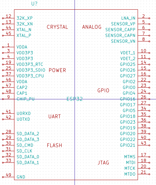
Notice that the component created is just a schematic view. It doesn’t have the footprint of the part to do the actual layout of the board. If the chip needs a custom footprint, it can be created in the footprint editor. I already have a footprint for the ESP32 (it’s a default QFN48), and opening it up in the footprint editor looks like this: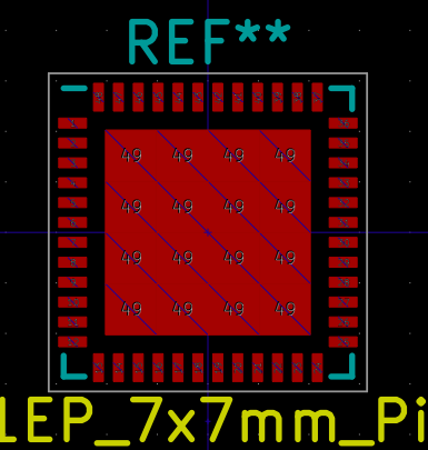
Notice that each pad on the footprint has a number on it. These match with the pin number created in the component. So pin 1 of the ESP32 (VDDA) matches with the upper left pin in the footprint.
After creating a component, I can begin laying out the full system schematic in the schematic editor. In here I can wire up the ESP32 to other chips, resistors, capacitors, etc.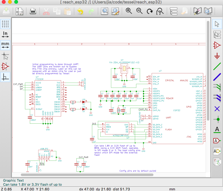
Schematic lines can be connected via a wire or just by naming multiple pins the same name. After laying out the schematic, I usually like to have a design review to catch any errors before I start laying out the PCB. The PCB layout process is pretty tedious and having to change a design results in a lot of lost time.
When the schematic is completed, I can then start laying out the PCB. I haven’t gotten to this part yet for this board.
All my custom components are kept in a library separate from KiCad’s default ones. I use Tessel’s Kicad Library since almost all my projects are related to Tessel.
Choosing other parts
I’m not using an ESP32 module for this design, just the bare bones chip. So I need to pick out the following main components:
- some sort of flash chip for extra space
- all the supporting circuitry to make the esp32 function
- figure out the programming method and if there’s anything I need to support it
The ESP32 also supports up to 8MB of SPI SRAM. I had a hard time finding any chips above a few hundred kb, and I also couldn’t find any reference designs of anyone doing it, so I decided not to include it in my design. Theoretically the SRAM could be connected to any of the other SPI busses as long as the software registers are configured properly. However, I couldn’t find any information on how to set up a SPI bus to be memory mapped as external RAM.
Flash
The datasheet says that the ESP32 supports 16MB of flash, so I went and selected Winbond’s W25Q128FVSIG. I’ve had success with using Winbond’s chips before for Tessel, and if things go wrong, I can always swap down to an 8MB flash chip like in the ESP32 reference design.
The Winbond flash supports multiple types of SPI communication: SPI, Dual SPI, and Quad SPI. Dual SPI operates 2-3x faster than normal SPI and quad SPI is 4-6x faster. Normal SPI has 1 pin that sends data (along with a clock pin and a chip select pin). Dual SPI increases the data transfer by repurposing pin as a data pin for a total of 2 data pins (usually called DI and DO), and quad SPI uses up another two pins (HOLD and WP).
The ESP32 seems like it supports quad SPI due to the way that the pins are named (SD_DATA 1 through 4), but even if it doesn’t I should be able to fall back to a slower SPI speed.
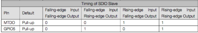
Also important to note is that there are different SPI modes depending on when data is read/written with respect to the clock pin. The Winbond flash supports SPI modes 0 and 3 (both modes are common). The ESP32 can select which SPI mode it wants to communicate to the external flash by pulling certain pins low or high. The default mode corresponds to SPI mode 0:
Supporting circuitry
There’s additional components needed for the following to ensure proper function of the ESP32:
- Crystal
- Voltage regulator
- USB to UART converter
- the wifi/bluetooth antenna
The crystal oscillator is a source for the ESP32’s system clock. The ESP32 can have up to 3 clock sources, an internal 8MHz oscillator, an external clock from 2MHz - 60MHz, and a real time clock of 32kHz (optional). I selected a 40MHz clock which is the same frequency as the reference design.
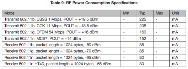
This dev board needs some way to draw power, and the easiest is usually via a USB port. But USB runs at 5V while the ESP32 needs 3.3V to operate, so the voltage regulator drops the 5V input to a 3.3V output. In addition, I also added a breakout pin so that an external LiPo battery can be hooked up. According to this Sparkfun post the ESP32 could only run sporadically off of a 200mA power supply, but ran fine with a LiPo that supported up to 1A draw. I doubt it’s using the full 1A, but according to the datasheet, the ESP32 can use 225mA during wifi transmit alone:
Assuming that the regular GPIO pins can also be drawing power during wifi transmission, I selected a voltage regulator that could supply up to 600mA. This is probably overkill since most USB ports only supply up to 500mA, but Digikey had a weird price range in which the 300mA, 600mA and 1A regulators were the cheapest…
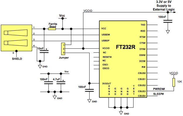
The Sparkfun post also mentions a USB to UART converter which is needed for programming the ESP32’s firmware. In the post they use an external breakout board, the FTDI basic. I just went ahead and included the FTDI chip in the design. The FTDI chip can output in both 5V and 3.3V, so it was important to make it 3.3V to match the ESP32. Luckily the FTDI data sheet shows how to set the chip to output in 3.3V by hooking up the 3V3OUT pin to the VCCIO pin.
The reference design for the ESP32 has the wifi/bluetooth antenna printed directly on the PCB. There’s a lot of voodoo black magic about designing PCB antennas, and I didn’t want to get into that on my first iteration of the board, so I went ahead and included a chip antenna. I choose the same antenna from Tessel 1. I’m not super concerned about the antenna right now, as long as the antenna pin isn’t grounded I should be able to get something out of the ESP32. I’ve had boards in which I’ve removed the antenna, cut it off, etc, and still work despite all that.
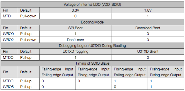
The ESP32 has 5 pins that are used to select the various boot modes. It’s important to make this configurable so that I can test different parts of the design later:
I also added in a lot of breakout pins so that I could get at almost any pin during the debug process. The first iteration of a board is designed for maximum testability. I want to figure out everything I can do on this board before having to make another revision.
Next step is laying out the board.